Passive FET Level Shifter
A few months ago while designing some JTAG/SWD level shifters, I learned about a low-cost bidirectional level shifter circuit topology which requires little to no power supply sequencing. It sounded too good to be true, but it turned out to be a fairly common trick, and it does have its tradeoffs.
Circuit topology
The circuit is based around a single transistor per channel, which could be a BJT or a FET, but I'll stick with FETs here to match commonplace implementations.
           VDDL                  VDDH
           ___                   ___
            |                     |
            |_________,           |
            |         |           |
           +-+        |          +-+
           | | Rl     |          | | Rh
           | |        |____      | |
           +-+       __ _ __     +-+
  IO_L _____|________|__^  |______|_____ IO_H
                       Q1
VDDL should be less than VDDH and the value of the pullup resistors Rl and Rh need to be selected based on the drive strength of the bus. Missing from the drawing is the FET's intrinsic diode, but this plays an important part in the circuit.
Circuit description
Since this is a bidirectional level shifter, there are several cases to consider. I won't consider cases involving both sides of the bus driving it to opposite levels, only the valid cases where one side is driving and the other is listening.
Case 1: IO_L drives low
If IO_L drives low, then Q1's gate is higher than its source, turning it on. This causes the FET to shunt IO_H to IO_L, following it to ground.
Case 2: IO_H drives low
If IO_H drives low, then Q1's intrinsic diode will be forward biased, shunting its source to IO_H, following it toward ground. As this happens, Q1's gate becomes higher than its source, turning it on harder and causing amplification. Thus, the bus current is still shared by the channel as well as the intrinsic diode, allowing IO_L to approach voltages far less than the diode's forward voltage above IO_H.
Case 3: IO_L drives high, or is left floating
Q1 is free to conduct current from IO_L through to IO_H until the voltage across its gate and source is lowered to its turn-off value. Once Q1 is off, IO_H is left to be overcome by Rh until it rises to VDDH.
Case 4: IO_H drives high, or is left floating
Similarly, Q1 is free to conduct current from IO_H through to IO_L until the voltage across its gate and source is lowered to its turn-off value. Once Q1 is off, the two sides of the bus will be isolated, and IO_L will remain pulled up to VDDL by Rl.
Benefits and trade-offs
It's a pretty nifty circuit, involving three jellybean parts per channel, and being fairly relaxed on power supply sequencing. According to Cases 3 and 4 above, it is agnostic of push-pull versus open-drain buses, supporting both cases. This makes it ideal for applications such as hotplugged I²C and other bidirectional buses.
This comes at a cost, however. There are two main design concerns when building with such a level shifter:
- Rise times can be heavily dependent on pullup resistor values and bus capacitance, even when driven by push-pull drivers. This depends on bus direction.
- Whatever drives the bus must be strong enough to sink current from both Rl and Rh pullup resistors.
Generally speaking, this is disadvantageous when compared to active level shifters which normally have a much higher input impedance.
Experiments
I got some small 4-channel discrete FET-based level shifter boards in order to run some experiments. The MOSFETs used are unlikely to be high performance, especially when compared with a dedicated IC such as the LSF0204 from TI which I plan to use on my JTAG/SWD level shifter up to a few dozen MHz.
There are 10 kΩ pullup resistors on each side of the FET to the respective VDD, and I used VDDL of 3.3 and VDDH of 5 V in my experiments. A fast edge from a 50 Ω source was used as stimulus, and the test was carried out on breadboard, so there is likely to be notable stray bus capacitance.
Push-pull considerations
At least at voltages above VDDL, the passive type of level shifter shown here will essentially convert even push-pull buses into an open-drain bus. Between states though, the rise times can still be somewhat faster than an equivalent open-drain bus. Recall that in cases 3 and 4, Q1 can remain on if the undriven side of the level shifter is at voltage lower than VDDL (assuming ideal VGSth).
For down-shifting, this would mean that the rise time would essentially remain unaffected since any voltage that IO_L can have is still lower than a high-driven IO_H. However there is a non-zero VGSth of about 1 volt on the FET, resulting in a RC curve between 2.3 and 3.3 V and a correspondingly slow 300 ns rise time (excuse the source ringing):
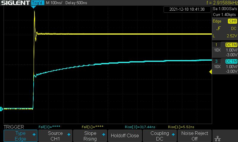
For up-shifting, the tradeoff is more apparent. IO_L can conduct current through Q1 to IO_H until both are at VDDL (assuming ideal VGSth). At this point, Q1 has to turn off, leaving the only way to continue to charge IO_H toward VDDH being Rh.
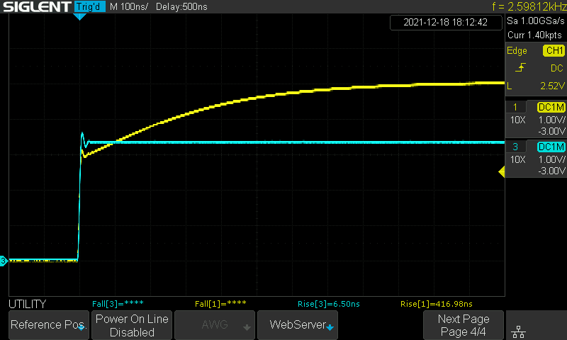
This causes a fast rise to just under 3 V, followed by a glacial RC curve the 2 remaining volts up toward VDDH.
There is scope to reduce the pullup values below 10 kΩ, depending on the capability of the drivers being put on the bus, but the existing value is a reasonable default. Without decreasing them, these specific devices are limited to bus rates of approximately 400 kHz assuming a "safe" pulse width three times longer than the 400 ns rise time.
Note that in both cases (and in the case of an open-drain bus), falling edges are generally unaffected as they transit through the level shifter assuming the driver has a drive strength far exceeding the bus current. Some distortion should be expected when downshifting on falling edges as Q1 turns on part-way through the edge once IO_H comes lower than VDDL in voltage.
Downshifting: 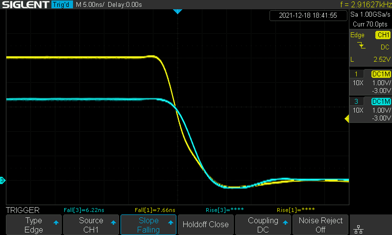
Upshifting: 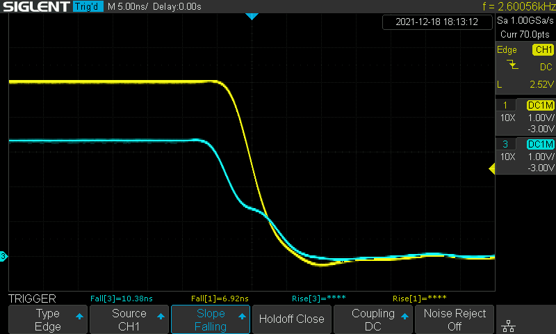
Conclusion
Passive bidirectional level shifters are an attractive option for their low external part count, low cost, and relative ease of supporting hotplugging. Even discrete MOSFETs can afford a cheap solution for buses such as fast-mode I²C and lower speed SPI buses.
Pushing the boundary on speed would require more careful part selection and layout considerations than my experiment with unknown-origin transistors soldered onto a breadboarded module, and I consider my measurements only educational and indicative rather than anything authoritative. Dedicated voltage level shifting families like the LSF family boast bus speeds up to 100–200 MHz, but this will be on extremely low capacitance buses and with very strong pullups. Still, I am looking forward to measuring the performance of the LSF0204 in my JTAG/SWD logic level shifter. It is amazing to see what this technology is capable of.
Perhaps it could be fun and insightful to do some more careful experimentation with building discrete level shifters. There's probably nothing revolutionary to discover but it could be an interesting rabbit hole.